AI-Assisted PCB Design Environment
An active PCB automation prototype that connects AI agents to EasyEDA Pro through MCP tools, with workflows for project inspection, part selection, schematic edits, PCB layout, routing checks, DRC feedback, and manufacturing-readiness review.
- Role
- Workflow design, tool integration, documentation, and validation strategy
- Stack
- EasyEDA Pro Desktop, MCP tools, Codex-style agents, local Ollama workflows
- Status
- Working automation prototype with growing smoke tests and visual QA outputs
Purpose
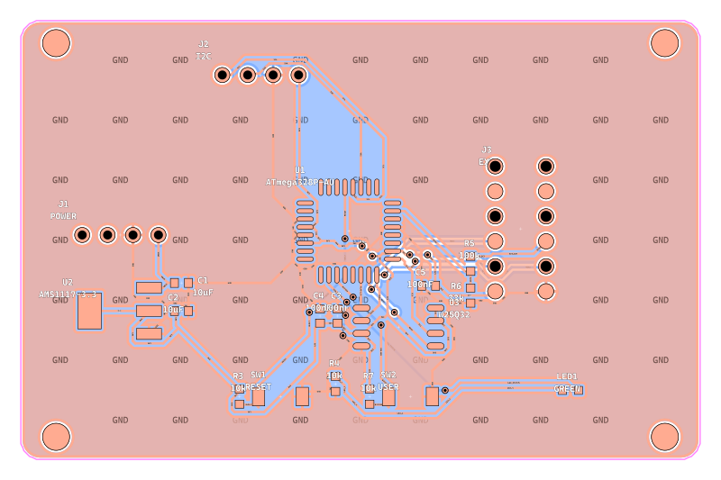
I am building this as a practical electronics-design assistant rather than a chat-only experiment. The goal is for an agent to inspect the active EasyEDA project, resolve verified parts, apply schematic or layout changes, run design checks, and report exactly what succeeded or failed from tool evidence.
Architecture
The workflow uses EasyEDA Pro Desktop as the live PCB editor, a customized EasyEDA extension to expose project and board operations, MCP tools for structured agent access, and a bridge layer for local Ollama model experiments. Launcher scripts and smoke tests help keep the local model profile, context window, tool schemas, and EasyEDA startup behavior consistent.
Validation
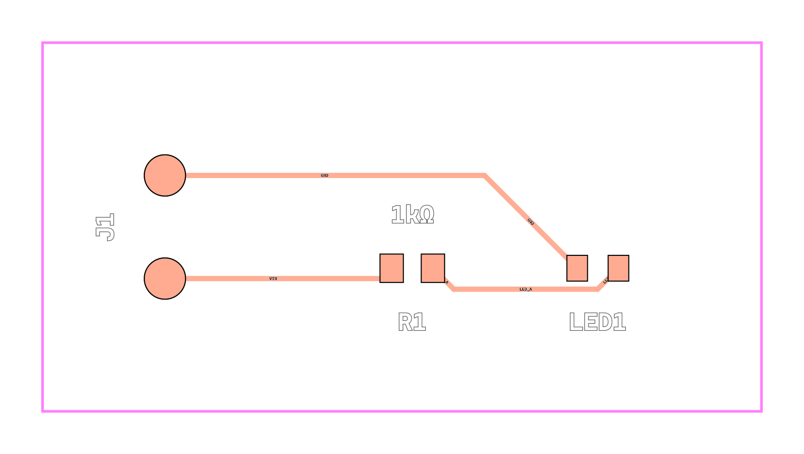
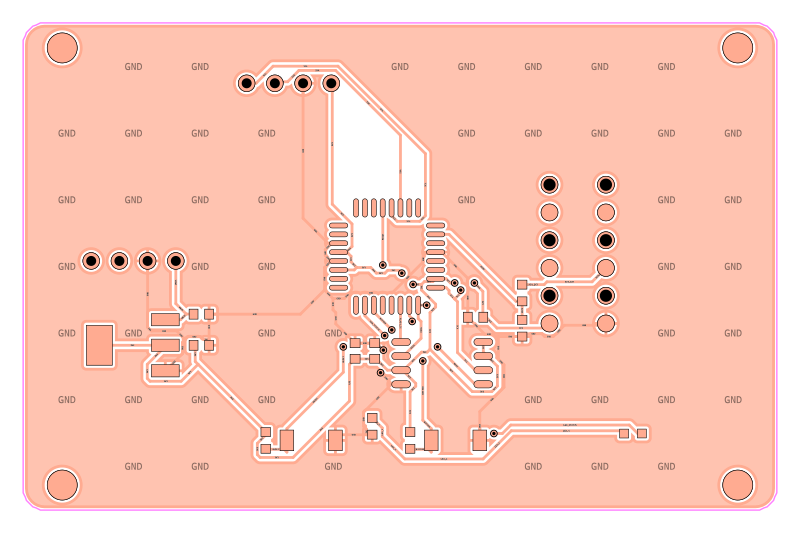
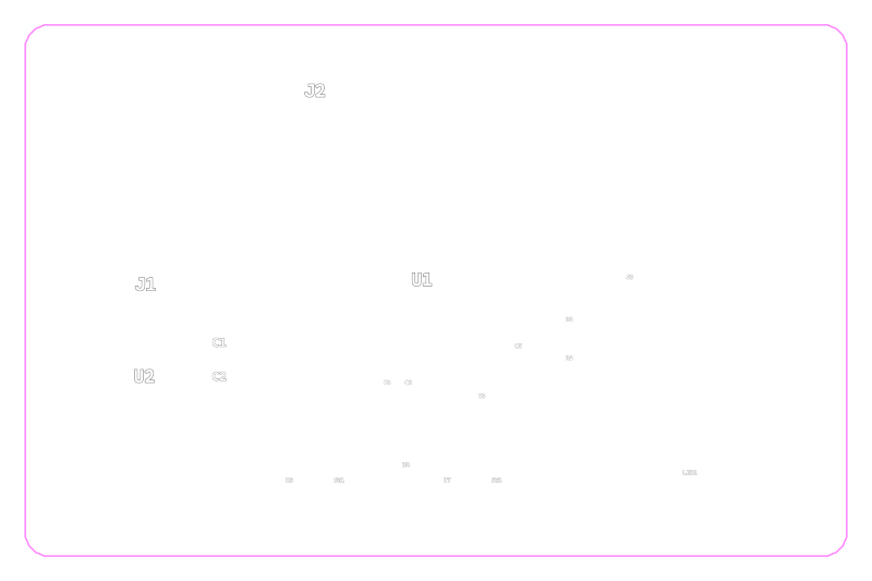
Current validation includes static release gates, local bridge smoke tests, compact tool-output checks, live MCP call tests, DRC/readback behavior, and visual manufacturing QA exports. I treat it as an active engineering automation project, not a fully reliable autonomous PCB designer or manufactured hardware product.
What It Demonstrates
This project demonstrates MCP-based control of a PCB editor, AI-assisted schematic and layout workflow design, local inference experiments for engineering tools, compact tool-output design for smaller models, DRC and manufacturing-readiness automation, and honest reporting around an evolving hardware/software toolchain.